Design Review Example

A behind-the-scenes look at a real PCB review

This is an example review we did for an internal project: a Multi Battery Charger PCB. Below you can see the type of feedback you can expect from us: concrete, substantiated, and focused on improvements that matter.

This is a translation of the original review in Dutch.

Schematic Review

General
Place a capacitor at every power input pin of every chip (U4 VCC, U4 Vref & Vdd, etc). 100nF or 1uF is fine. When a chip switches fast, it needs a short pulse of current. Traces act as inductors, causing voltage to drop without sufficient capacitance near the chip (can cause noise or EMC issues).
Footprints for capacitors: 0603 is fine, but for larger values (> 1uF) make sure to:
  • specify a voltage rating (add a 'rating' field in the component). Suggestion: >=50V for 24V components, >= 16V for 5V components.
  • select a footprint that exists (e.g. 10uF@50V probably doesn't exist in 0603, may need 0805, 1206 or 1210)

Tip: signals without net labels are not easily recognizable in the layout. Where needed, you can add net labels in your schematic to make layout work easier.

Op-amp
TC75S67TU,LF unfortunately has a very limited input signal range (0-1.4V). We should look for a 'rail to rail' op-amp. For example TLV9001. The symbol for it is already in KiCad libraries.
Datasheet excerpt showing limited input range
Datasheet shows limited input range of 0-1.4V
Power the op-amp from 5V instead of 3.3V (input signal goes up to 4.2V!)
Fuel Gauge
Give input resistors a precision rating. I would choose 0.1% (with 1% of 8.4V you're already 84mV off).
Q6+R19 are not really needed, this only saves ~6uA according to the datasheet. I would leave them out (leave SW unused).
D2 is connected backwards. This is a zener diode (which conducts current in 'reverse direction' above a certain voltage). The BZX84C4V7 seems like a suitable variant (more specific part number for the 4.7V variant).
To be safe, I would place a DNP resistor from +3.3V to U2 pin 6. If needed, we can solder a 0-ohm there with the prototype (instead of regulator circuit Q5/D2/R18).
5V DC-DC
5V DC/DC: double-check the connection diagram. I think the voltage divider for the 
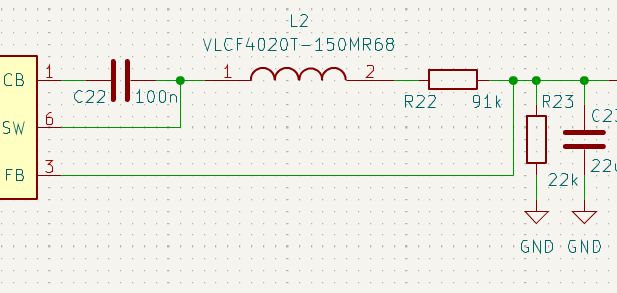
FB pin is not correct. Compare with datasheet section 9.2
Datasheet reference design for DC-DC
DC-DC converter schematic with incorrect voltage divider
Vin capacitors: if C18-C20 are indeed available in 0603, C21 can be removed (if not, update C18-C20 footprints and place the smallest footprint closest to U3 in layout).
Battery Charger
Vref is an output, so don't connect it to 3.3V (note this is a small error in the symbol, vref should ideally be defined as a power output)
PG pin will always be low in practice, so D5 might eventually be removed. Optionally keep it for now (debug?)
Double-check the connection diagram. Compare with datasheet 10.2.2 or 10.2.1 and pay attention to the SRN, SRP lines and component RSR1. I would take a bit more space in the schematic (put it in a subsheet) and try to place the components more clearly like in the datasheet.
Battery charger reference schematic
Battery charger schematic with points of attention
CE pin should connect to the other microcontroller GPIOs instead of vref if possible. That way we still have the option to turn charger(s) on/off in software. If there aren't enough pins, you can share them per 2 packs.

Charger: there's a capacitor on CE. I think it belongs on VREF:

Capacitor placement issue
Capacitor placement needs to be corrected
Battery Connector
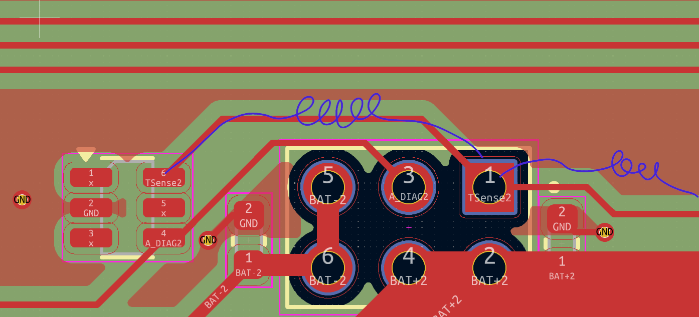
A_DIAG1 is now connected with 10K to ground. This becomes a voltage divider together with the 2M series resistor in the pack, so remove it! For EMC you could add a small capacitor (e.g. 22-50pF).

Better idea: ESD protection on the battery connector is a good idea, because the user can touch it and/or static zaps can occur when plugging/unplugging. Suggestion: component ESDA6V1-5SC6 (in KiCad library). This component also has about 50pF of capacitance as a side benefit, so it can work as both an EMC filter and ESD protection.

I would connect both Tsense and A_DIAG1 to one of the pins of the ESD chip (choose depending on what's convenient in layout).
ESD protection component
Add a 0603 capacitor footprint (10nF or optionally DNP) to GND for BAT+ and BAT-.
24V Power Connector

We still need to choose this, keep enough space in your layout. I think there will also be a fuse or input filter added.

Op-amp input resistor: I would remove the bypass of R53 and make it a 10K by default. The 10K can help as extra input protection for ESD and can then be easily replaced with another value if desired without having to cut a trace.
Input resistor recommendation
Recommendation for input resistor
Extra: Test Points

It can be useful to add some test points. In the schematic you can add a 'testpoint' symbol on signals you would want to measure during verification. Just see where it fits in the layout, doesn't have to be on every signal. The simplest footprint I often use is TestPoint:TestPoint_Pad_D1.0mm.

Layout Review

Power Input
Calculate maximum current, also useful to note in the schematic. Worst-case I think 6x3A * 8.4V / (24V * 90% efficiency)?
Let's add a fuse at J1. You can use this footprint: Jitter_Footprints:Fuse_2410_6125Metric. Component can be one from the Bel Fuse 0679H0250 series (choose value slightly above maximum current).
The Vin trace should be quite a bit wider, something like 5mm I think (you can use the KiCad Calculator). Especially the first section where all current flows.
Fuel Gauge
Still an error in the schematic. The datasheet is particularly unclear/misleading here. After comparing reference designs and devkits, my conclusion is that the text is correct but you can't trust all the pictures. The confusing thing is that this chip should not be directly connected to GND (very unusual):
  • Pin 7: CSN. Connect only this one to board ground
  • Pins 8,9,15 (CSPL/GND/EP): all connect together to BAT-
  • Decoupling capacitor (C92) between REG and BAT-
Fuel gauge layout example
Example layout from the datasheet (p29)

This chip effectively has its own local 'ground' that is only connected to the rest of the board through the sense resistor. I would normally never recommend this but this is apparently how this chip is designed.

Layout tip: I think after the above changes, the sense resistor rotated 180 degrees would work out better. That would also make the BAT- trace shorter.
Battery Connectors
BAT- should be wider. The same current flows through here as through BAT+!
ESD protection (e.g. D31) is already nicely close to the connector, but I would route the traces further away from other signals so the ESD pulse doesn't 'jump over' or interfere.

Tip: the pins on the ESD protection chip are interchangeable, if it's convenient for your layout you can also use other pins (doesn't have to be pin 4/6).

ESD: important to actually route the signal through the protection chip for ESD, suppressing high-frequency pulses works less well if it's on a 'siding'. Think of the traces as inductors:
ESD routing issue
Current routing vs. desired routing for ESD

I would do something like this (as an example):

Recommended ESD routing
Copper Pours (GND planes)
Set clearance smaller, e.g. 0.2mm is sufficient. Then the gaps and edges around traces & vias become much smaller.
Set 'pad connections' to 'reliefs for PTH' for best heat dissipation for SMD components (charger IC etc).
Charger Circuit
Decoupling capacitor is in the right place, could optionally be even closer.
Current charger layout

An example of how I would do this part:

  • Pay attention to the power flow: it runs along the capacitor, then with a short connection directly to the chip
  • Vias at the GND side of capacitors for a low-inductance connection to the GND plane on layer 2
  • In places where the PCB will get hot (like at this chip), you can place some extra vias to add more copper + conduction to the GND planes ('thermal vias' as they're often called)

Recommended charger layout
Recommended charger layout with thermal vias
Same for the REGN capacitor, ideally you would prioritize this in the layout over the resistor block (those can also move a bit to the left).
REGN capacitor placement
General

Things to check after all other changes:

Sufficient GND vias:
  • at every GND pin (so there's always a short route to the ground planes on layer 2/3)
  • GND return vias near (groups of) traces that switch layers
  • 'stitching vias': connect all GND planes regularly, e.g. every 10-20mm and at corners of a plane. So the planes don't act as antennas (resonate at high frequency)
Silk screen: remove or neatly position designators
Silk screen: text/label at connectors and a PCB name+version number
Add 3D footprints so we can properly fit the PCB in an enclosure
Current Sense

This is more of a tip, current layout is good enough. I expect the charging current will be a few % lower than expected because of this, but that's not that precise anyway.

Perhaps educational because this comes up often: measuring currents using a series resistor. If you want to do this accurately, it's best to use 'Kelvin style' (four-terminal sensing). This is something you can't easily indicate in the schematic, so something to always pay extra attention to in the layout.

As an example: the charger chip measures charging current by measuring the voltage drop across RSR1. Current flows in the direction of the blue arrows, and thus sees some resistance from the copper in addition to RSR1. The most accurate is to route a separate pair of traces (shown in green) directly from the resistor to the chip, without sharing them with e.g. the voltage feedback network:

Kelvin sensing layout
Kelvin-style current sensing layout

Want this kind of feedback on your design?

We look at your PCB with experienced eyes and help you find problems before they become expensive.

See our Design Review service