As a PCB designer, the so-called ‘ground plane’ is your best friend. It makes layout easier, improves EMC performance, and as a bonus you get increased signal integrity. But be careful to keep the ground plane intact.
Ideally, the ground plane should be kept solid. No holes, cutouts, slots, or gaps. See this previous post about current loops for an explanation of why this is important.
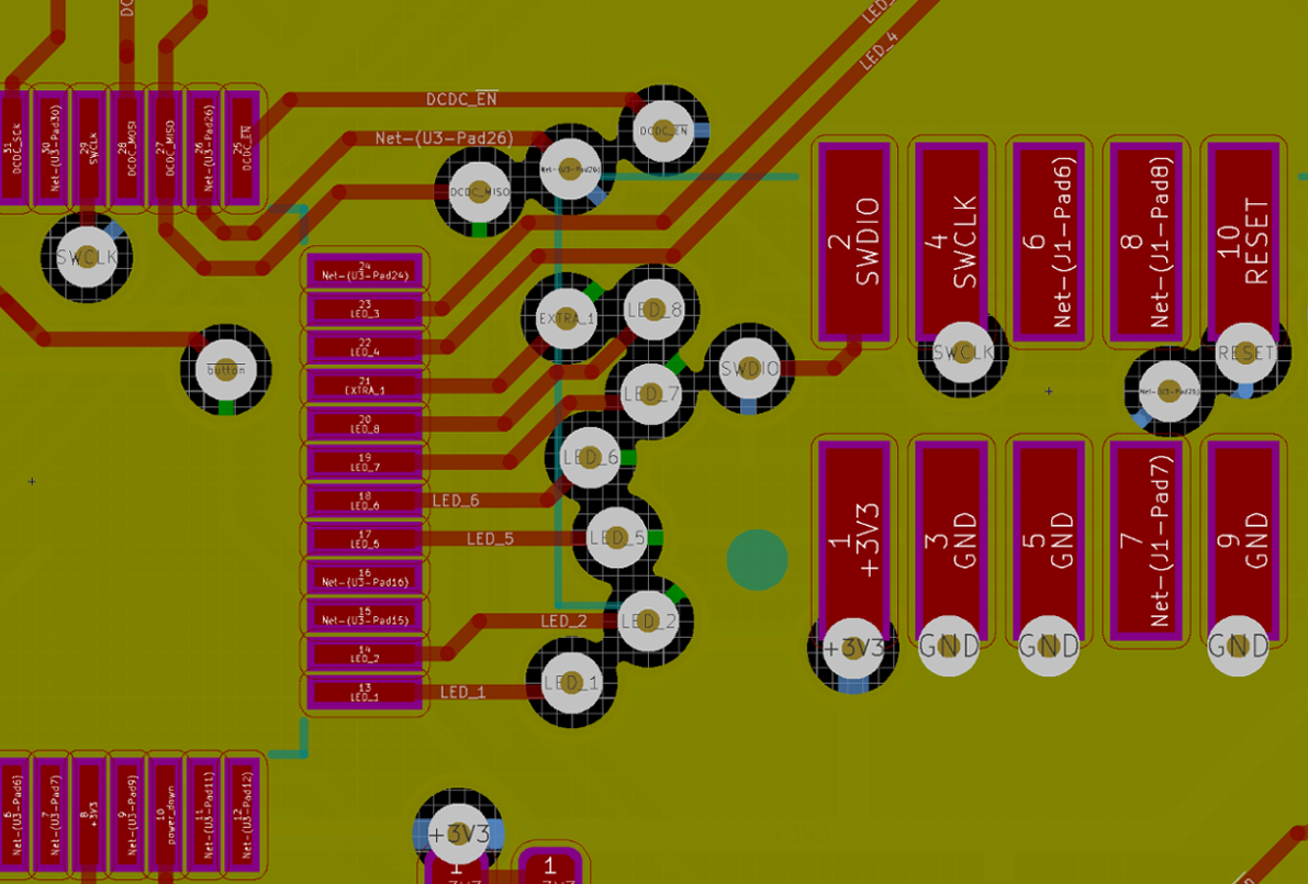
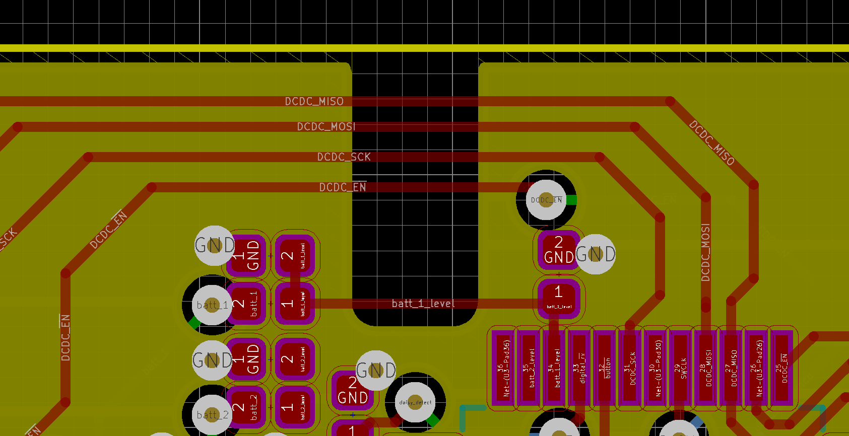
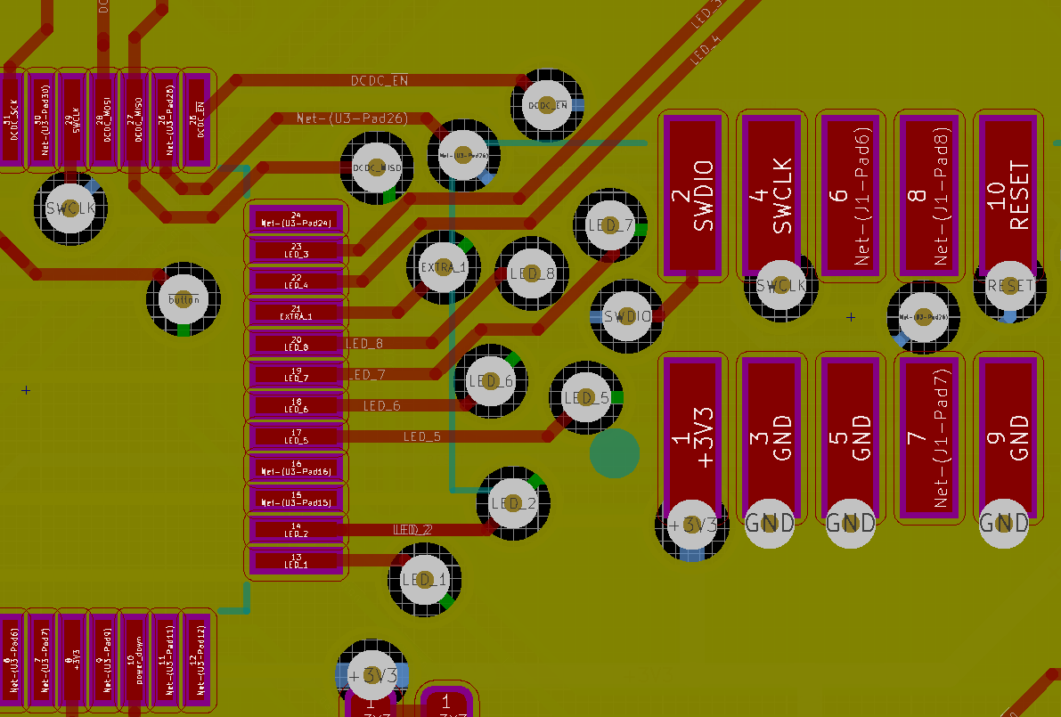
One perfectly solid ground plane sounds nice, but it’s not very practical. Vias, for example, create holes in the ground plane. Luckily they are super tiny, so in practice, we tend to ignore them. But real boards don’t have just one via. Some designs will have thousands of them!
What happens if you place a lot of vias too close together? It is no longer a bunch of small holes: you have accidentally created a slot in the ground plane!

You can avoid this issue by following two simple steps:
Especially if your design is very dense, you may not reach perfection. This is OK as long as you are aware of the tradeoff you are making. That’s what engineering is about!
Hopefully, this tip helps you design even better circuit boards. If you have any questions about this topic, don’t hesitate to contact me at pcbdesign@jitter.company.
Want to feel confident that your board will work right the first time? Curious for feedback on your design? Have a look at our PCB design check service!